Manual Focus Nikon Glass
p.2448 #1Manual Focus Nikon Glass
Oh My, that second one.... ha ha ha. and the first one, windy a bit, eh?
DeltaSigma wrote:
Hyde Park, London
28mm/2.8 AI-S
https://live.staticflickr.com/65535/54460128319_d210ab69a8_h.jpgDSC_5314 by Colin McIntosh, on Flickr
https://live.staticflickr.com/65535/54460201568_ea8805cda8_h.jpgDSC_5357: Mature BMxers by Colin McIntosh, on Flickr
https://live.staticflickr.com/65535/54459132532_1617ea318b_h.jpgDSC_5338: Hyde Park, London by Colin McIntosh, on Flickr
Colin
Apr 19, 2025 at 07:20 AM
p.2448 #2Manual Focus Nikon Glass
I ALMOST bought a pre-planted pot of Peonies yesterday, but decided against it, my black thumb will kill anything lately, including hostas.  I'll just enjoy other people's flowers.
SiMuMe wrote:
https://www.cimeza.com/stuff/fpic/20250418_Df_55339D.jpg
Nikkor-H 85mm f/1.8 + Df | F5.6
I'll just enjoy other people's flowers.SiMuMe wrote:
Apr 19, 2025 at 07:24 AM
p.2448 #3Manual Focus Nikon Glass
Oh my, I can hear the waves and it's making me homesick.
BLLX wrote:
These are with DF + 28/2.8 ai-s
https://live.staticflickr.com/65535/54454052846_432e31f43d_b.jpg
DF_20250413_BLX_4749.jpg by -Morten-, on Flickr
https://live.staticflickr.com/65535/54453205172_b70db3aff6_b.jpg
DF_20250413_BLX_4746.jpg by -Morten-, on Flickr
https://live.staticflickr.com/65535/54454412695_c98149b45c_b.jpg
DF_20250413_BLX_4759.jpg by -Morten-, on Flickr
Apr 19, 2025 at 07:26 AM
p.2448 #4Manual Focus Nikon Glass
Hi, everyone:
James, terrific work on the film cameras. On another front, very creative as usual with the microscope photography.
Colin, great street shots. I have said it before, you are darn good at it.
Siphiwe, very nice colors with the DF.
Morten, congrats on the new lens. nice looking rig.
I will do my best to take decent photos at the Easter Parade tomorrow.
From 2024:

Fuji S5 + 50mm f/2 Ai
Serge
James, terrific work on the film cameras. On another front, very creative as usual with the microscope photography.
Colin, great street shots. I have said it before, you are darn good at it.
Siphiwe, very nice colors with the DF.
Morten, congrats on the new lens. nice looking rig.
I will do my best to take decent photos at the Easter Parade tomorrow.
From 2024:
Fuji S5 + 50mm f/2 Ai
Serge
Apr 19, 2025 at 07:37 AM
p.2448 #5Manual Focus Nikon Glass
Thanks Serge.
Are you going to wear an Easter bonnet too?
serge07 wrote:
Hi, everyone:
James, terrific work on the film cameras. On another front, very creative as usual with the microscope photography.
Colin, great street shots. I have said it before, you are darn good at it.
Siphiwe, very nice colors with the DF.
Morten, congrats on the new lens. nice looking rig.
I will do my best to take decent photos at the Easter Parade tomorrow.
From 2024:
https://live.staticflickr.com/65535/54462026449_05ecbf7fbb_h.jpg
Fuji S5 + 50mm f/2 Ai
Serge
Apr 19, 2025 at 09:31 AM
p.2448 #6Manual Focus Nikon Glass
Working in the semiconductor industry SEMs were a staple tool to help debug chip failures.
I wasn't a failure analysis engineer but those guys had lots of really cool tech at their disposal. I used to hate being informed about field failure from certain customers knowing there would be immense time pressure to find the root cause of the problem - Hey, you are selling us 100 million devices a year and we have one failure after it has been in the field for 6 months...... don't make us stop our production lines. Having said that I used to relish the challenge (from a chip designer's perspective) to help find the issue and pacify the customer. SEM helped a lot, as did FIB (focused ion beam) work. Imagine etching a 0.2um trench thru your diatom so you could see inside.
Colin
James Markus wrote:
That's impressive.
Scanning Electron Microscope next Jim?Colin, I was driven to it by the culture taking a turn into chaos. I need order, facts, truth, and love to breath. One place laws remain unchanged are diatoms who live in geometric marvel glass houses. Feeding birds and squirrels - these are ways for me to look at the world with the distopian crap stripped away. If I could afford an electron microscope I would use it.
Jim
I wasn't a failure analysis engineer but those guys had lots of really cool tech at their disposal. I used to hate being informed about field failure from certain customers knowing there would be immense time pressure to find the root cause of the problem - Hey, you are selling us 100 million devices a year and we have one failure after it has been in the field for 6 months...... don't make us stop our production lines. Having said that I used to relish the challenge (from a chip designer's perspective) to help find the issue and pacify the customer. SEM helped a lot, as did FIB (focused ion beam) work. Imagine etching a 0.2um trench thru your diatom so you could see inside.
Colin
James Markus wrote:
DeltaSigma wrote
James Markus wrote
My first diatom. The Nikon N Plan 10x/0.30 0.17 microscope objective paired with the Nikon CF PL 2.5x photo relay eyepiece lens = 25x in color or colour and b&wScanning Electron Microscope next Jim?
Jim
Apr 19, 2025 at 10:02 AM

p.2448 #7Manual Focus Nikon Glass
DeltaSigma wrote:
Working in the semiconductor industry SEMs were a staple tool to help debug chip failures.
I wasn't a failure analysis engineer but those guys had lots of really cool tech at their disposal. I used to hate being informed about field failure from certain customers knowing there would be immense time pressure to find the root cause of the problem - Hey, you are selling us 100 million devices a year and we have one failure after it has been in the field for 6 months...... don't make us stop our production lines. Having said that I used to relish the...Show more →That's impressive.
Scanning Electron Microscope next Jim?Colin, I was driven to it by the culture taking a turn into chaos. I need order, facts, truth, and love to breath. One place laws remain unchanged are diatoms who live in geometric marvel glass houses. Feeding birds and squirrels - these are ways for me to look at the world with the distopian crap stripped away. If I could afford an electron microscope I would use it.
Jim
A boyhood friend's little brother Eric sat on their living room floor with a hammer and bashed the family bake-a-lite radio into little pieces. The mother and father were theater actors - always sing Frank Sinatra tunes - blew a gasket. "Why, Why did you do that?" Eric calmly said; "I wanted to meet the little people inside the radio." That's tenacious curiosity, and I never forgot it.
Hunting down the root cause of a failure is something I really can appreciate, and I hope this doesn't horrify you. However, in light of the Eric story - I decided I wanted to meet the little people inside a burnt out Pentium III 866 mhz cpu. When I read up on how to properly open it up, and it taking days to weeks to free the silicon - I got out my hammer, and kitchen blow torch, and got my look see within minutes. If I wanted to see entire cores beautifully photographed I can go to Apple's site anytime. This was me looking with my primitive biological Leica compound microscope, and an adventure. I hope your chip designer sensibilities aren't too upset, but it literally was trash from my perspective. Torched outside, utility knife flick, 6000 grit sand paper left over from refinishing a tub, some safe mild acids, and a quick bath in an ultrasonic cleaner late (about 15-20 minutes) I got this
https://www.fredmiranda.com/forum/topic/1898739/
I couldn't tell what part is what, but you could. It is amazing that human's make such small complicated switches/transistors - and much smaller now-a-days.
Working in the semiconductor industry SEMs were a staple tool to help debug chip failures.
I wasn't a failure analysis engineer but those guys had lots of really cool tech at their disposal. I used to hate being informed about field failure from certain customers knowing there would be immense time pressure to find the root cause of the problem - Hey, you are selling us 100 million devices a year and we have one failure after it has been in the field for 6 months...... don't make us stop our production lines. Having said that I used to relish the...Show more →
James Markus wrote
DeltaSigma wrote
James Markus wrote
My first diatom. The Nikon N Plan 10x/0.30 0.17 microscope objective paired with the Nikon CF PL 2.5x photo relay eyepiece lens = 25x in color or colour and b&wScanning Electron Microscope next Jim?
Jim
A boyhood friend's little brother Eric sat on their living room floor with a hammer and bashed the family bake-a-lite radio into little pieces. The mother and father were theater actors - always sing Frank Sinatra tunes - blew a gasket. "Why, Why did you do that?" Eric calmly said; "I wanted to meet the little people inside the radio." That's tenacious curiosity, and I never forgot it.
Hunting down the root cause of a failure is something I really can appreciate, and I hope this doesn't horrify you. However, in light of the Eric story - I decided I wanted to meet the little people inside a burnt out Pentium III 866 mhz cpu. When I read up on how to properly open it up, and it taking days to weeks to free the silicon - I got out my hammer, and kitchen blow torch, and got my look see within minutes. If I wanted to see entire cores beautifully photographed I can go to Apple's site anytime. This was me looking with my primitive biological Leica compound microscope, and an adventure. I hope your chip designer sensibilities aren't too upset, but it literally was trash from my perspective. Torched outside, utility knife flick, 6000 grit sand paper left over from refinishing a tub, some safe mild acids, and a quick bath in an ultrasonic cleaner late (about 15-20 minutes) I got this
https://www.fredmiranda.com/forum/topic/1898739/
I couldn't tell what part is what, but you could. It is amazing that human's make such small complicated switches/transistors - and much smaller now-a-days.
Apr 19, 2025 at 11:03 AM
p.2448 #8Manual Focus Nikon Glass
DeltaSigma wrote:
Thanks Serge.
Are you going to wear an Easter bonnet too?
James, terrific work on the film cameras. On another front, very creative as usual with the microscope photography.
Colin, great street shots. I have said it before, you are darn good at it.
Siphiwe, very nice colors with the DF.
Morten, congrats on the new lens. nice looking rig.
I will do my best to take decent photos at the Easter Parade tomorrow.
From 2024:
https://live.staticflickr.com/65535/54462026449_05ecbf7fbb_h.jpg
Fuji S5 + 50mm f/2 Ai
Serge
It is under serious consideration.
Serge
Thanks Serge.
Are you going to wear an Easter bonnet too?
serge07 wrote
Hi, everyone:James, terrific work on the film cameras. On another front, very creative as usual with the microscope photography.
Colin, great street shots. I have said it before, you are darn good at it.
Siphiwe, very nice colors with the DF.
Morten, congrats on the new lens. nice looking rig.
I will do my best to take decent photos at the Easter Parade tomorrow.
From 2024:
https://live.staticflickr.com/65535/54462026449_05ecbf7fbb_h.jpg
Fuji S5 + 50mm f/2 Ai
Serge
It is under serious consideration.
Serge
Apr 19, 2025 at 02:17 PM
p.2448 #9Manual Focus Nikon Glass
NightOwl Cat wrote:
I ALMOST bought a pre-planted pot of Peonies yesterday, but decided against it, my black thumb will kill anything lately, including hostas. I'll just enjoy other people's flowers.
How cold does your area get, Laura? Clearly not cold enough here as they were tried in 2023 but died off. Give them a short, at least you'll know you tried.
I ALMOST bought a pre-planted pot of Peonies yesterday, but decided against it, my black thumb will kill anything lately, including hostas.
I'll just enjoy other people's flowers.How cold does your area get, Laura? Clearly not cold enough here as they were tried in 2023 but died off. Give them a short, at least you'll know you tried.
Apr 20, 2025 at 01:15 AM
p.2448 #10Manual Focus Nikon Glass
DeltaSigma wrote:
Working in the semiconductor industry SEMs were a staple tool to help debug chip failures.
I wasn't a failure analysis engineer but those guys had lots of really cool tech at their disposal. I used to hate being informed about field failure from certain customers knowing there would be immense time pressure to find the root cause of the problem - Hey, you are selling us 100 million devices a year and we have one failure after it has been in the field for 6 months...... don't make us stop our production lines. Having said that I used to relish the...Show more →
Needs a big-eyed emoji. That sounds very interesting, Colin.
Apr 20, 2025 at 01:18 AM
|
p.2448 #11Manual Focus Nikon Glass
BLLX wrote:
New AF lens - shot with MF (55/2.8 micro ai-s)
https://live.staticflickr.com/65535/54460763322_bd2c92d677_b.jpg
DF_20250419_BLX_4826.jpg by -Morten-, on Flickr
https://live.staticflickr.com/65535/54460763222_3bd745e0fb_b.jpg
DF_20250419_BLX_4823.jpg by -Morten-, on Flickr
Nikon must make more of these small form factor lenses. They are lovely to use on these small mirrorless bodies. The only improvement I'd like on the 40 is to have a little more resistance on the focus ring. Otherwise, lens is great. Enjoy it.
Apr 20, 2025 at 01:23 AM
p.2448 #12Manual Focus Nikon Glass
It can get quite cold here, though lately not as cold as the first year we were here, Jan of 1994 we had two straight days of -25°F/-32°C. With the hostas, those were the third attempt, they lasted me about three years, dying off slowly. I'm done.
I've never had peonies though.
SiMuMe wrote:
I'll just enjoy other people's flowers.How cold does your area get, Laura? Clearly not cold enough here as they were tried in 2023 but died off. Give them a short, at least you'll know you tried.
I've never had peonies though.
SiMuMe wrote:
NightOwl Cat wrote
I ALMOST bought a pre-planted pot of Peonies yesterday, but decided against it, my black thumb will kill anything lately, including hostas. I'll just enjoy other people's flowers.Apr 20, 2025 at 10:13 AM
p.2448 #13Manual Focus Nikon Glass
To keep things ticking over I am adding a few wider field of view images.
All from Hyde Park, London, 16x9 crop and 28/2.8 AI-S
 DSC_5370: Hyde Park, London by Colin McIntosh, on Flickr
 DSC_5367 by Colin McIntosh, on Flickr
 DSC_5365 by Colin McIntosh, on Flickr
Colin
All from Hyde Park, London, 16x9 crop and 28/2.8 AI-S
DSC_5370: Hyde Park, London by Colin McIntosh, on FlickrDSC_5367 by Colin McIntosh, on FlickrDSC_5365 by Colin McIntosh, on FlickrColin
Apr 20, 2025 at 10:28 AM
p.2448 #14Manual Focus Nikon Glass
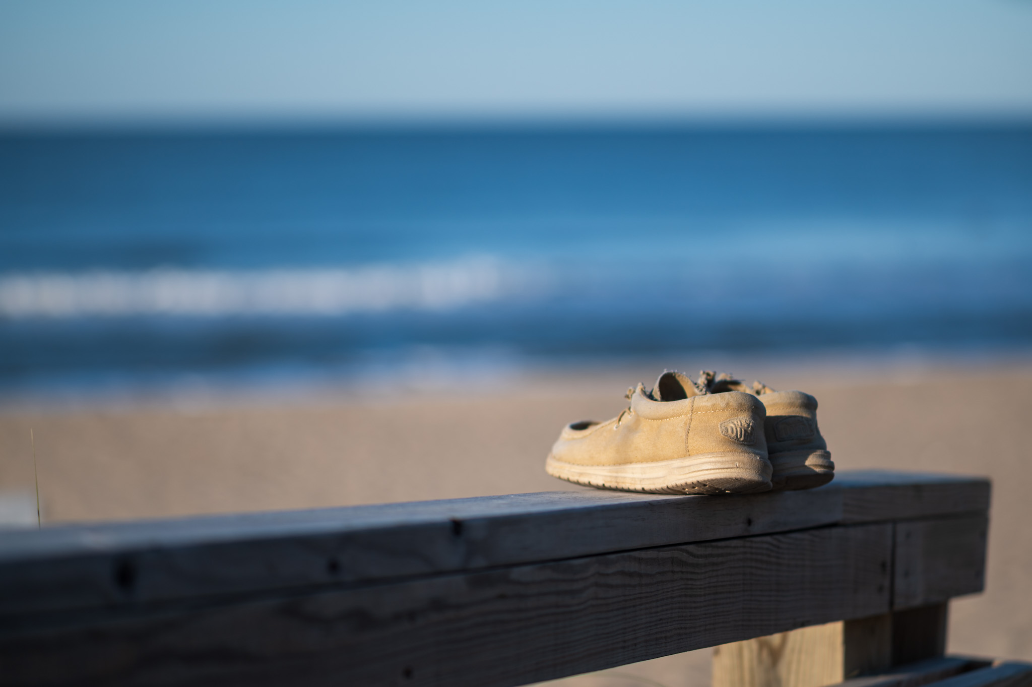
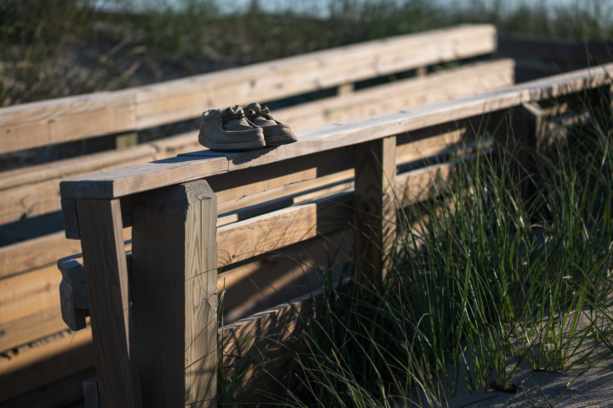
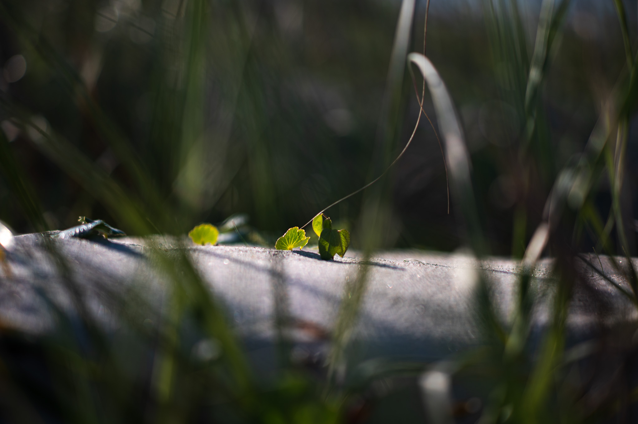
Been busy but shooting a little. Playing with the 105mm f/2.5 at the beach (as always).
Apr 20, 2025 at 01:36 PM
p.2448 #15Manual Focus Nikon Glass
How about these, Siphewe?

SiMuMe wrote:
I wasn't a failure analysis engineer but those guys had lots of really cool tech at their disposal. I used to hate being informed about field failure from certain customers knowing there would be immense time pressure to find the root cause of the problem - Hey, you are selling us 100 million devices a year and we have one failure after it has been in the field for 6 months...... don't make us stop our production lines. Having said that I used to relish the challenge (from a chip designer's perspective) to help find the issue and pacify the customer. SEM helped a lot, as did FIB (focused ion beam) work. Imagine etching a 0.2um trench thru your diatom so you could see inside.
ColinNeeds a big-eyed emoji. That sounds very interesting, Colin.




SiMuMe wrote:
DeltaSigma wrote
Working in the semiconductor industry SEMs were a staple tool to help debug chip failures.I wasn't a failure analysis engineer but those guys had lots of really cool tech at their disposal. I used to hate being informed about field failure from certain customers knowing there would be immense time pressure to find the root cause of the problem - Hey, you are selling us 100 million devices a year and we have one failure after it has been in the field for 6 months...... don't make us stop our production lines. Having said that I used to relish the challenge (from a chip designer's perspective) to help find the issue and pacify the customer. SEM helped a lot, as did FIB (focused ion beam) work. Imagine etching a 0.2um trench thru your diatom so you could see inside.
Colin
Apr 21, 2025 at 06:43 AM
p.2448 #16Manual Focus Nikon Glass
I will follow along with Colin and post my contribution for the week. No IR converted camera, but IR filter on monochrome sensor.
Nikkor 2.8cm f/3.5 LTM mount lens.
George
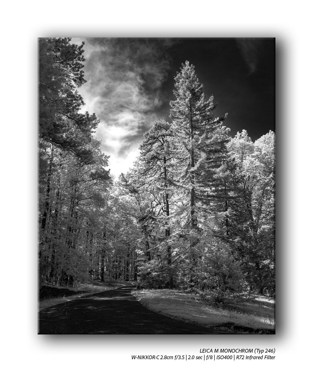
Nikkor 2.8cm f/3.5 LTM mount lens.
George
Apr 21, 2025 at 05:44 PM
p.2448 #17Manual Focus Nikon Glass
Warrior of Capestrano, 6th century BC (National Archaeological Museum of Abruzzo, in Chieti).
Does this statue depict a Italic king or a woman?? read:
https://www.preistoriainitalia.it/en/2021/01/01/il-guerriero-di-capestrano-e-una-donna/
Nikon Z6 w/Nikkor AI 50/1.4 at f/4, 1/50 s, 1000 ISO
Nikon Z6 w/Nikkor AI 50/1.4 at f/5.6, 1/50 s, 2500 ISO
Edited on Apr 22, 2025 at 02:34 AM · View previous versions
Does this statue depict a Italic king or a woman?? read:
https://www.preistoriainitalia.it/en/2021/01/01/il-guerriero-di-capestrano-e-una-donna/
 |
||
 |
||
|
|
||
 |
||
|
Edited on Apr 22, 2025 at 02:34 AM · View previous versions
Apr 22, 2025 at 02:24 AM
p.2448 #18Manual Focus Nikon Glass
55/2.8 macro
The bluebells are in full swing at the moment.
I screwed up the aperture. I thought I was at f/11 but must have knocked in whilst leaving the path.
Not enough DoF and mid-day flat light wasn't the best. Excuses out of the way.
 NZ8_0374: Bluebells by Colin McIntosh, on Flickr
The bluebells are in full swing at the moment.
I screwed up the aperture. I thought I was at f/11 but must have knocked in whilst leaving the path.
Not enough DoF and mid-day flat light wasn't the best. Excuses out of the way.
NZ8_0374: Bluebells by Colin McIntosh, on FlickrApr 22, 2025 at 02:34 AM
p.2448 #19Manual Focus Nikon Glass
NightOwl Cat wrote:
It can get quite cold here, though lately not as cold as the first year we were here, Jan of 1994 we had two straight days of -25°F/-32°C. With the hostas, those were the third attempt, they lasted me about three years, dying off slowly. I'm done.
I've never had peonies though.
Peonies need up to 40 days of less than 4 deg C(~39F) temperature to flourish. We have maritime climate and it never gets that cold here. So, I understand why they didn't thrive.
Apr 22, 2025 at 05:28 AM
p.2448 #20Manual Focus Nikon Glass
NightOwl Cat wrote:
How about these, Siphewe?
" Imagine etching a 0.2um trench thru your diatom so you could see inside.", that what needs the second emoji.
How about these, Siphewe?
" Imagine etching a 0.2um trench thru your diatom so you could see inside.", that what needs the second emoji.
Apr 22, 2025 at 05:30 AM